NE555 is the most popular integrated circuit (IC) for time related circuits, for example- generating square waves, tones, clock pulses, time delay, PWM signals, etc. It is used in most digital and analog circuits. The Basic 555 timer circuit diagram and its working are explained in this article. it is invented in 1971 by an American company Signetics. A standard 555 chip includes 25 transistors, 15 resistors, and 2 diodes. It has 8 pins; the pin description of this IC is given below.
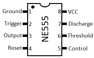
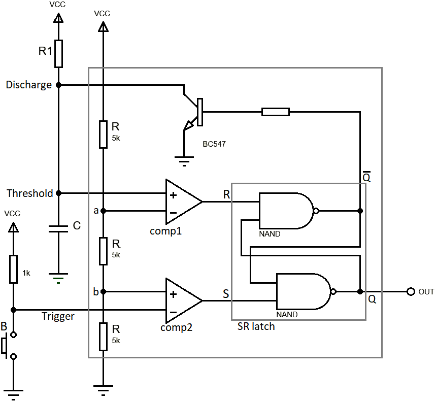
Ground and VCC are the power pins. The output pin goes high when the voltage on the trigger pin is below VCC and it is low when the voltage on the threshold pin is above two-thirds of VCC. By the control pin, we can adjust the threshold voltage. Here is the internal block diagram.
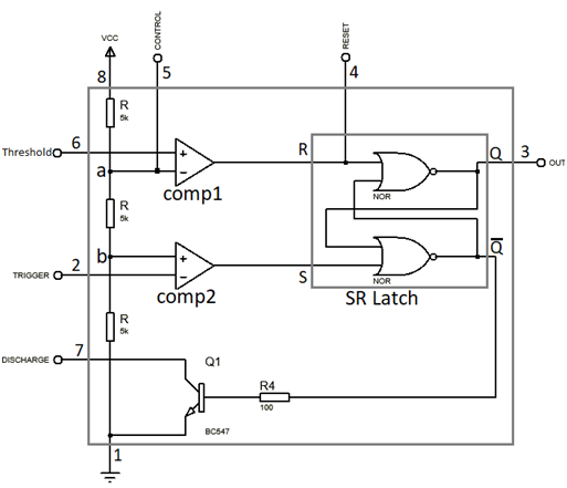
As you can see there are three resistors connected in series between VCC and ground. That creates two junctions between them that are ‘a’ and ‘b’. The potential on junction ‘a’ is two-third of VCC and on junction ‘b’ is one-third of VCC.
The ‘a’ junction is connected to inverting input of the first comparator and also with the control pin of IC and the ‘b’ junction is connected to the non-inverting input of second comparator. Non-inverting input of first comparator is threshold pin and inverting input of the second comparator is trigger pin. Outputs of both comparators are connected with a set-reset pin of an SR latch. There are three modes of operation of the 555 chip.
Table of Contents
1. 555 timer circuit for astable output (555 in astable mode)
When the output of a 555 IC is not stable and it continuously changes between high and low states then it is in astable mode.
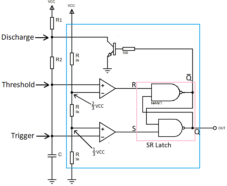
In the figure, the internal 555 timer circuit diagram is shown under the blue rectangle and all circuit out of the blue rectangle is an external circuit. Resistors R1, R2, and capacitor C are connected in series.
At the initial state (at time t=0), the output of the second comparator is high because the voltage on the trigger pin is less than one-third of VCC, and the latch is set, so the output of IC is high. Capacitor C starts charging through resistors R1 and R2 and the potential difference across capacitor is increasing gradually.
When this potential difference reaches above 2/3 of VCC, the comparator goes low and when this voltage reaches near 1/3 of VCC then the output of the second comparator goes high. This phenomenon resets the latch and Q output goes low and inverted Q goes high. The transistor whose base is connected to inverted Q is now in on condition. Now current from VCC is flowing through R1 and transistor. The capacitor is discharging through resistor R2 and transistor. When the charge on the capacitor remains one-third of VCC, the second comparator goes high and latch sets.
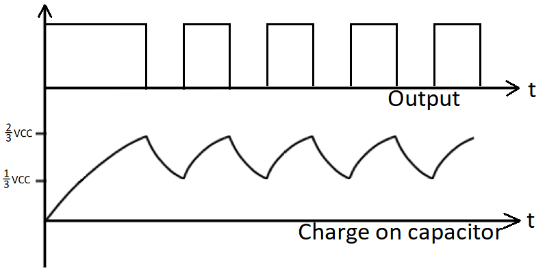
This process is continuous and we get a perfect square wave.
We can adjust the transition speed and frequency by changing the value of resistors and capacitors.
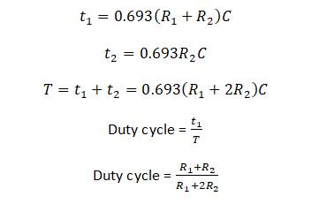
In this case duty cycle of output will be always more than 50%, because the capacitor will charge through both R1 and R2 resistors and it will discharge through only resistor R2. To get a 50% duty cycle we can use this circuit.

In this circuit, the capacitor will charge through resistor R1 and diode because of lower resistance than R2 and it will discharge through R2. So, to get 50% duty cycle resistor R1 and R1 should be equal.
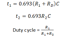
If R1>R2 (duty cycle > 50%)
If R1<R2 (duty cycle < 50%)
So, we can use this circuit as a PWM signal generator by replacing R1 and R2 with a potentiometer.
2. 555 timer circuit for monostable output (555 in monostable mode)
In this mode one state of output is stable. We will see the circuit of 555 whose low state is stable. Applications of 555 in monostable mode are generating time delays, frequency division, switching the relays, etc.
In the above circuit, the output is initially low because the voltage on the trigger pin is greater than one-third of VCC, and voltage on the threshold pin is less than two-third of VCC.
Therefore, the output of the first comparator is high and the second comparator is low. So, reset the pin of latch triggers. Since inverted Q output is high, the transistor is on state and current from VCC is flowing through R1 and transistor BC547 to the ground. As we press the button ‘B’, the voltage at the trigger pin becomes zero, and the output of the second comparator goes high, set pin of latch triggers and its outputs interchange, therefore the output of IC is high.
Now, the transistor is in an off state and the capacitor starts charging through resistor R1. As the voltage on the threshold reaches near two-third of VCC, the second comparator goes high, and latch triggers reset again. Transistor has turned on again and current from VCC is flowing through R1 and transistor to ground and capacitor is also discharging through the transistor.
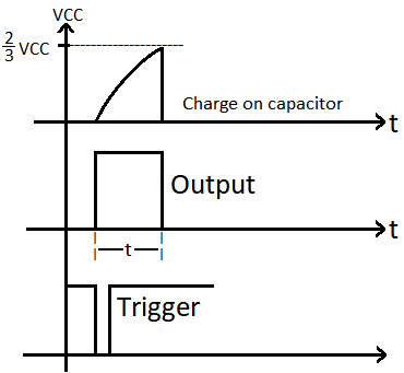
t = 1.1R1C
3. Bistable mode
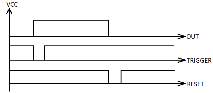
When both output states of the 555 timer circuit diagram are stable then it is called the bistable mode of 555 timer IC.
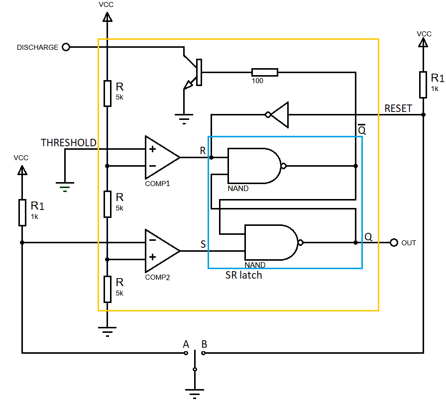
In this circuit, we don’t need any capacitor for charging and discharging purposes. We only need to access the SR latch, actually, we can design the circuit by using the SR latch only. By setting and resetting the latch we will get the desired output. For accessing the reset pin of the latch we will use the reset pin of IC and for accessing the set pin of latch we will use the second comparator that means trigger pin of IC. Both reset and trigger pin is pulled high. Therefore, the output of the second comparator and output of the NOT gate is low.
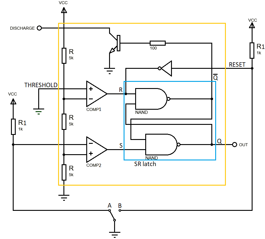
But as we complete the ‘A’ circuit with the ground using a switch, the voltage at the trigger pin becomes zero, and the output of the comparator goes high. So, the Set pin of latch triggers and output of IC goes high.
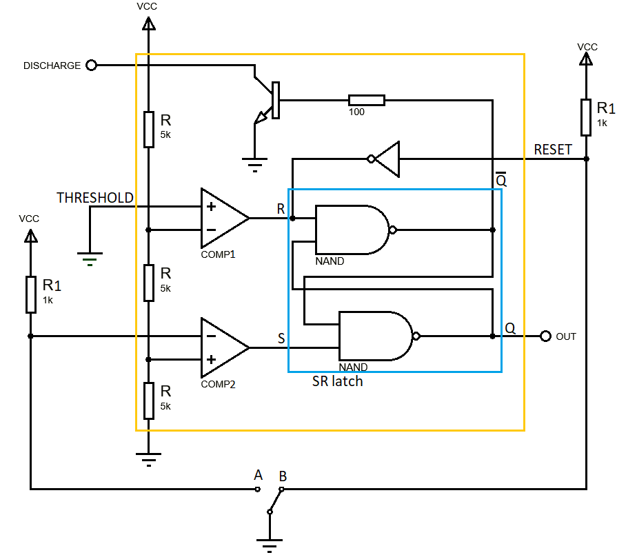
And as we complete ‘B’ circuit voltage at reset pin of IC is zero. Therefore, the output of the NOT gate goes high, and reset pin of latch triggers, and output of IC goes low.
Applications of 555 timer IC
The 555 Timer circuit diagram can be found in most digital or electronics circuit boards. Since it is very popular in clock and time delay circuits. some popular applications are following.
- To generate PWM (pulse width modulation) and PPM (pulse position modulation) signal
- It provides accurate time delays
- Schmitt triggers
- To design timer Switch
- DC voltage regulator
- Square wave generator
- Triangular wave generator
- Tone generator
Buy 555 timer IC on amazon
| Amazon link for India | Amazon link for other countries |
|---|---|
I’m not sure where you’re getting your info, but great topic. I needs to spend some time learning much more or understanding more.
Thanks for great info I was looking for this information for my mission.