Buck boost converter is a DC to DC converter. A DC to DC converter converts the voltage levels of DC sources. We call it DC to DC converter because it take DC voltage as input and gives also DC voltage as output. I have published two separate project articles on buck converter and boost converter each with detailed explanation on working principle, circuits and applications. First read those article because that will give a clear scope of vision to better understand this project. Buck boost converter is a combined circuit of buck converter and boost converter as the name sounds. You can get an idea about working principle of buck boost converter yourself by understanding the working principles of buck and boost converter individual.
Table of Contents
A real world example of where you may need a buck boost converter
Let’s say you have powered a 12 volt electronics device with 12 volt battery. But problem is that a 12 volt battery sometimes gives 13 volt in case of fully charged and drops down to 11 volt in case of fully drained. In this case sensitive devices may get damage. Here we have to use two converters, first is buck converter if voltage is above 12 volts and second is boost converter if voltage is below 12 volts. But how will it be that we add both functionality in one circuit. In this project we will see that how we can design such circuit which can perform both functions. Let’s connect both circuits in series.
There are many unused component in this circuit. So, after removing the filter capacitors C1 and adding inductor L1 and L2 in series, we get this
Circuit diagram shown above is non-inverting buck/boost converter. Here by controlling both switches in a proper manner we can use it as buck/boost converter. If SW2 is open SW1 control the buck functionality and when SW1 is closed then SW2 controls boost functionality. In this circuit we have to control two switches. But there is a circuit available in which we have to care about only one switch. We call this circuit inverting buck-boost converter or flyback converter.
Inverting buck-boost converter or flyback converter
Let’s understand the modes of working principle of inverting buck boost converter or flyback converter circuit.
Mode-1:- in this mode switch is on and inductor is storing energy. Diode D is off.
Switch ON, Duty cycle (D) =
TON = DT
(VL)ON = V
Mode-1:- in this mode switch is off and inductor is releasing its energy. Capacitor C is charging reversely. This is why we call this converter an inverting converter.
Switch OFF
TON = (1-D)T
(VL)OFF = -VO
Mode-1:- in this mode switch is off and diode D is also off. Capacitor voltage appears across output. This voltage is negative.
As per volt-sec rule, voltage across inductor
(VL)ONTON+ (VL)OFFTOFF = 0
V(DT) + (-VO)(1-D)T = 0
VD = VO(1-D)
Example –
D = 0.6
VO = V(0.6/0.4)
VO = (3/2)V (Boost mode)
In actual buck-boost converter switch is replaced with MOSFET and it is driven by a PWM pulse.
For a stable output voltage at any load we need to change the duty cycle every time when we change the load. Otherwise at different load output voltage will also be different at fix duty cycle. For this we need to design such switcher circuit and give it output feedback so that it can adjust its duty cycle.
Generating the PWM pulse for boost converter
There exists many specific IC for switching. But for better understanding first we will see how we can create such circuit without any premade IC. For this we will use op-amp and comparators. But before that we will see how we can generate the PWM signal.
Logic for generating the PWM pulse is same as we saw in the buck converter and boost converter project. In the waveform you can see that we triangle signal is compared with feedback voltage. Here output voltage is inverted so we can’t connect it directly to comparator. We have to connect a differential op-amp to calculate the difference of output voltage and a reference voltage. Output of differential op-amp is feedback voltage. Where triangle voltage is greater than feedback voltage output of comparator is low. So, triangular signal is connected to inverting terminal of comparator and feedback is connected with non-inverting terminal of comparator.
Now if output voltage decrease then feedback voltage will increase. Then duty cycle of comparator will increase, so the output voltage will increase then feedback voltage will decrease. This way output voltage stabilizes itself according to different loads. So, this increment and decrement of output voltage continues. This is why if you observe the output voltage is never smooth of any buck/boost converter.
Circuit diagram of boost converter
If you observe the working diagram of inverting buck-boost converter, we have to use P-channel MOSFET as switch. But, channel resistance of P-channel MOSFET is way higher than N-channel MOSFET. To use N-channel MOSFET we have to change the position of switch.
To make whole circuit without existing IC, we need following component.
- MCP602 op-amp
- mos
- Potentiometer
- Capacitors
- TL431 transistor for reference voltage
- MOSFET driver (TC4420)
- MOSFET (IRL540)
- Inductor
- Diode
As you can see the circuit looks very messy, complex and took a large space. This is why we don’t prefer this circuit.
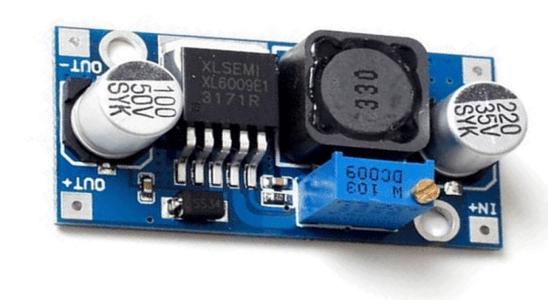
Now we will design the buck converter using a specific IC for buck-boost converter. For this circuit we need following component.
- XL6009 DC-DC step up/down converter IC
- Capacitors (47uF and 470uF)
- Inductor (100uH)
- Diode
- Potentiometer (100k)
MOSFET switch is integrated in the IC. You can see how simple this circuit is looking. Just a few components compared to previous circuit. Its efficiency is also good compared to previous circuit. This is why this circuit is preferred. Don’t forget to use heat sink with the IC.
Applications of boost converter
- To regulate the power supply
- Used in battery power systems
- It is used in power amplifiers
I realized more new things on this weight loss issue. 1 issue is a good nutrition is extremely vital whenever dieting. A massive reduction in bad foods, sugary food items, fried foods, sweet foods, red meat, and whitened flour products could be necessary. Holding wastes parasitic organisms, and toxins may prevent ambitions for losing weight. While selected drugs for the short term solve the issue, the unpleasant side effects are usually not worth it, and in addition they never offer you more than a short-term solution. This is a known indisputable fact that 95 of celebrity diets fail. Many thanks for sharing your opinions on this site.
I would like to thank you for the efforts you’ve put in writing this blog. I’m hoping the same high-grade blog post from you in the upcoming also. Actually your creative writing skills has encouraged me to get my own site now. Really the blogging is spreading its wings rapidly. Your write up is a great example of it.