In the project of dc dimmer circuit we saw that how we can step down the voltage using PWM. But in that circuit there is a problem of high voltage peak. That can destroy the sensitive electronics devices. For that kind of electronics devices there is another step down circuit called buck converter. Buck converter is a DC to DC step down converter. That means it converts any DC voltage to lower DC voltages. It doesn’t affect power much more so current will step up. We can use it in computer SMPS (switch mode power supply) to step down main supply to power the USB, DRAM and CPU (1.8V to 4.2V).
Table of Contents
Working of buck converter
It works on switching principle (PWM). The switching frequency is very high so that another energy storing element can be kept small. Let’s see the working circuit of buck converter. This circuit is extended version of PWM dimmer circuit. Inductor prevent that high voltage spikes which occurs in the PWM dimmer circuit.
Using figure above we will understand the working principle of buck converter. Here diode is used to discharge the inductor. Otherwise it will create a negative high voltage spike across switch. The switch (CH) is used in circuit is called chopper. In the actual buck converter circuit it is replaced with transistor. The capacitor is used to smooth out the output voltage.
When chopper is on then current starts rising and inductor will start creating its magnetic field and when chopper is off then this magnetic field will start collapsing, this will create a voltage difference across the inductor which will keep the current flowing through the load.
Before the energy of inductor is completely empty, we switch the chopper on again. This way we step down the supply voltage.
By changing the switching duty cycle of chopper we can change the output voltage.
Let’s see some graph of switching.
You can see in the waveform when chopper is “on”, output voltage (VO) is equal to supply voltage, inductor current (IL) is rising, diode current is zero, input current is rising and capacitor is charging as well.
When chopper is “off” then output voltage is zero, inductor current is decreasing, diode current flowing and then decreasing, input current is zero and capacitor is discharging.
When chopper is ON
VL(ON) = VS – VO
IC(ON) = IL – IO
When chopper is OFF
VL(OFF) + VO = 0
VL(OFF) = -VO
IC(OFF) = IL – IO
Applying voltage secondary balance
VL(ON) ´ TON + VL(OFF) ´ TOFF = 0
(VS –VO)´DT + (-VO)´(1-D)T = 0
VO = DVS
Here value of duty cycle is between 0 to 100%. So, this type of chopper shows the step down chopper.
Buck converter switching circuit
As we know that switching is very important for buck convert to work. We need an additional circuit for switching that can change it duty cycle also. Because if we change the loads at the same duty cycle, output voltage will also be different for different loads. So we need to provide output voltage feedback to the switcher circuit so that it can adjust it PWM for different current demand. There exists many IC’s for switching purpose.
First we will see how we can create such circuit without any premade IC. For this we will use op-amp and comparators. But before that we will see how we can generate the PWM signal.
In the waveform you can see that we triangle signal is compared with feedback voltage. Where triangle voltage is greater than feedback voltage output of comparator is high. So, triangular signal is connected to non-inverting terminal of comparator and feedback is connected with inverting terminal of comparator.
Now if output voltage decrease then feedback voltage will also decrease. Then duty cycle of comparator will increase, so the output voltage will increase then feedback voltage will also increase. This way output voltage stabilizes itself according to different loads. So, this increment and decrement of output voltage continues. This is why if you observe the output voltage is never smooth of any buck/boost converter.
Circuit diagram of buck converter
We can design the circuit diagram of buck converter using two methods. First we can design the whole circuit as shown or we can use existing IC. To make whole circuit we need following component.
- MCP602 op-amp
- Resistors
- Potentiometer
- Capacitors
- MOSFET driver (TC4420)
- MOSFET (IRL540)
- Inductor
- Diode
- TL431 (Voltage reference transistor)
Figure shown above is the circuit diagram of buck converter without using any premade switching IC.
Here feedback voltage is difference of a reference voltage and output voltage. So, it basically tells that output voltage is how much different from target voltage. If output voltage will increase then feedback voltage will decrease and if output voltage will decrease then feedback voltage will increase. So, as we discussed earlier that feedback voltage should connect to inverting terminal is got reversed. As you can see the circuit looks very messy, complex and took a large space. This is why this circuit is not preferred.
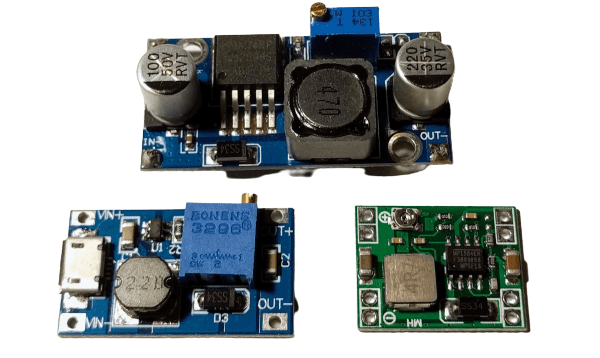
Now we will design the buck converter using a specific IC for buck converter. For this circuit we need following component.
- LM2576 DC-DC step down converter IC
- Capacitors (100uF and 1000uF)
- Inductor (100uH)
- Diode
- Potentiometer (100k)
MOSFET switch is integrated in the IC. You can see how simple this circuit is looking. Just a few components compared to previous circuit. Its efficiency is also good compared to previous circuit. This is why this circuit is preferred. Don’t forget to use heat sink with the IC.
Applications of buck converter
- In computer SMPS
- To drive LED array
- In telecom and data interface system