In this project you will learn how to make a digital counter display which will show you number of pulse applied to its clock pulse. This counter will count up to 999 but you can add more digits to increase count number. We will see this circuit using BCD counter and 7-segment hex decoder first then we will use CD4026 and 7-segment display for this. You can use the CD4026 alternative that is CD4033. These chips are 5 stage Johnson decade counter with decoded output which convert Johnson count (code) into 7-segment decoded output. This decoded output drives one stage (one numerical digit) in a 7 segment display.
So let’s see this circuit using counter and 7-segment display decoder.
This is the circuit of the 7-segment display circuit which will count up to 999 and it can count down also. To make this circuit count down counter display you have to pull down pin 10 of all counter IC which is responsible to count up or down.
Table of Contents
How this circuit works
Now let’s see how this circuit works. In this circuit there are three main components which are 4 stage BCD (binary coded decimal) counter, BCD to 7-segment decoder IC and 7-segment display. BCD counter will count up to 9 in binary and then reset to 0. When it reach to 9 then it pull carry out (CO) pin to low and then reset to high.
This carry out signal is used to give the signal to count up the next counter connected in cascaded mode. This IC can count down as well. We will see more details of this IC in Pin description. Then 7 segment decoder will decode that BCD counting into 7 segment display code which will show us the decimal equivalent of that BCD.
We have cascaded three stages of decoder circuit. Next stage will count up or down after previous stage is reset to 0 again since carry out of previous stage is connected to carry in of next stage. This way we can cascade as many digits as we want.
We have used CD4510B as BCD counter and SN74247 as BCD to seven segment decoder IC. Click on 7-segment hex decoder if you want detailed information on it.
CD4510B BCD counter
CD4510B is a BCD up/down counter which will count up to 9 in binary. This counter consists 4 synchronous clocked D type flip flop (with a gating structure to provide t-type flip flop capability). Let’s see the pin description of this IC.
Let’s see what every pins of this IC does. There are four outputs and four inputs. P1….P4 are the parallel inputs which are used to give the count value parallelly. Q1….Q4 are the output where the counting happens in binary. Preset enable is used to put the count value which is available at parallel input to the output. Carry in and carry out is used to cascade multiple counters. Carry out of least significant digit to carry in of more significant digit. Clock and all other control pin are common in cascading. Vss and Vdd are use to power the chip.
A high pulse on reset pin will reset the chip to the 0. Up/Down pin is used to either count up or count down. If this pin is pulled high then counter will count up and if this pin is pulled low then counter will count down. Every rising edge on clock pin will cause to count up or down of counter.
CD4026B: introduction
CD4026B consists of a 5-stage Johnson decade counter and an output decoder which converts the Johnson code to a 7-segment decoded output for driving one stage of a numerical display.
This chip is particularly designed for display application where low power dissipation and/or low power package count are important.
Pin diagram of CD4026B
CD4026B has 16 pin including 7 segment pins for 7-segment display, clock, reset (MR), clock inhibit (INH), display enable in (DEI), display enable out (DEO), carry out, ungated “c” segment out (UCS) and power pins. Let’s see the pin diagram of CD4026B.
Let’s briefly see the pin description of CD4026B.
Clock: – Here we provide the clock. At every rising edge of clock pulse, output segments will be set as it can draw next number on 7-segment display.
Clock inhibit: – This is an active high pin which ignore the clock if it is high.
Display Enable In: – This pin is used to enable or disable the display outputs. It enables the output when it is high.
Display Enable Out: – This pin pass the signal which is on “display enable in” to next chip in cascading.
Carry out: – This used in cascading of multiple CD4026B. This pin is usually high but when counting goes up to 9 then it goes low and when count resets to 0 then this pin goes high again. That means it gives the clock signal to next CD4026B after every time it counts from 0 to 9. It simply divides the clock be 10.
a…..g, UCS: – These pins are for 7-segment display.
Reset: – It resets the counting to 0.
VSS: – Power supply ground (0 volts).
VDD: – Power supply positive volt.
Features of CD4026B
- Counter and 7-segment decoding in one package
- Fully static counter operation: DC to 6 MHZ at VDD = 10 volt
- Ideal for low power displays
- Schmitt-triggered clock input (useful in sensored clock)
- Standardized, symmetrical output characteristics
Logic diagram of CD4026B
Let’s see the internal logic diagram of CD4026B.
As you can see that it has a 5 stage Johnson counter and a decoder circuit that decodes the count into 7-segement output for display equivalent count number.
CD4026B application
- Decade counter 7-segement decimal display
- Frequency division 7-segment decimal display
- Clocks, watches, timers (%60, %12)
- Counter/display driver for meter application
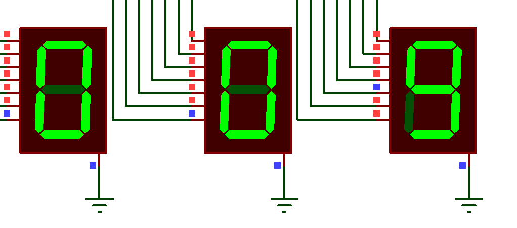
Circuit diagram for digital counter display using CD4026B
In this circuit three CD4026B chips and three 7-segment displays are used which will show us three digit decimal number. CD4026B is cascaded to show 10’s and 100’s places. This will together make a digital counter display.
We need these components to implement this circuit.
- CD4026B (number of chips will be same as decimal digits you want. In my case 3)
- 7-segment display (as digit you want)
Let’s see the circuit diagram of digital counter display.
Here as you can see that in this circuit three CD4026B is cascaded. Carry out pin is connected with clock input of next chip. You can add as many as you wish. First chip (U1) is driving display for 1’s place, second chip is for 10’s place and third chip is used to drive the display for 100’s place.
DEI (display enable in) is given to first chip and then it is given from previous DEO (display enable out) to next chip. Reset pins of all chips are individually tied to ground. You can tie them together and rest the counting form one button or something.
Use common cathode 7-segmetn display. Connect all segment (a…g) pin of CD4026B to segment pins of 7-segment display correctly. Connect common cathode to ground.
On the clock signal you can connect any type of sensor which can give a clock pulse in response to an event. So that you can count how many times that event occurred.