Unlike encoder which converts its 2N input lines into N digits binary number according to input line which is on logic high, digital decoder decodes that encoded N digit binary number and turns an output line high out of its 2N output lines corresponding to that binary number. It is also a combinational circuit and has ‘N’ number of line and 2N number of outputs. It turns one of these output high corresponding to code present on its inputs.
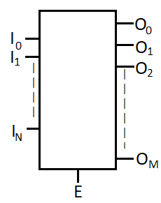
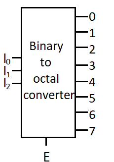
The picture shown above is a block diagram of decoder with ‘N’ number of input and ‘M’ number of output. Relation between input and output is M = 2N. ‘E’ is the enable pin.
Table of Contents
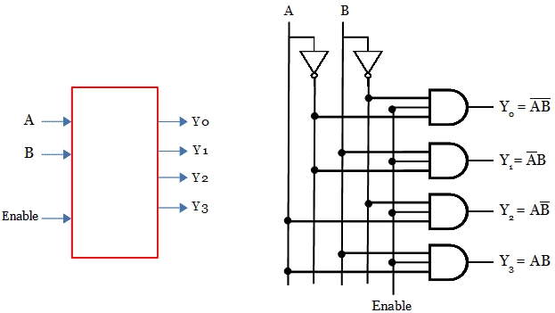
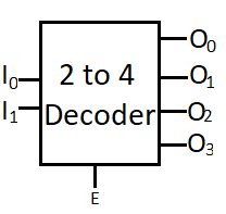
2×4 digital decoder
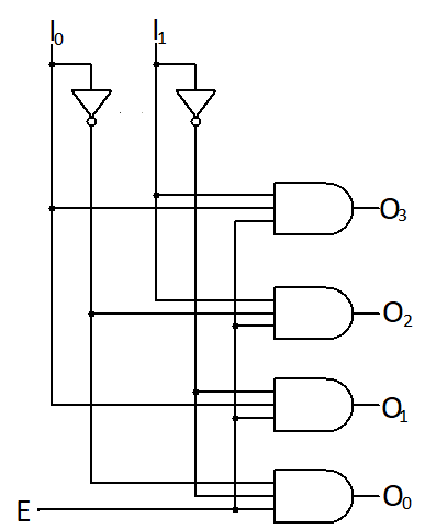
It has 2 inputs and 4 outputs. It will turn one of that four output high according to what is on the input.
Truth table of 2×4 decoder
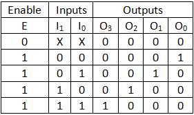
Now we can write the Boolean function using the truth table:
O3 = E.I1.I0
O2 = E.I1.I0’
O1 = E.I1’.I0
O0 = E.I1’.I0’
These functions are having product term so, we can use AND gates for implement it. Implementation of logic circuit for 2×4 decoder:
Binary to octal converter (3×8 digital decoder)
A 3 to 8 decoder has 3 inputs and 8 outputs. It is also called as binary to octal converter because it takes three bit binary input and gives output at any one pin out of 8 pins.
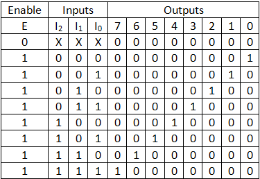
Truth table for binary to octal converter (3×8 decoder)
Boolean function:
7 = E.I0.I1.I2
6 = E.I0’.I1.I2
5 = E.I0.I1’.I2
4 = E.I0’.I1’.I2
3 = E.I0.I1.I2’
2 = E.I0’.I1.I2’
1 = E.I0.I1’.I2’
0 = E.I0’.I1’.I2’
Logic diagram implementation:
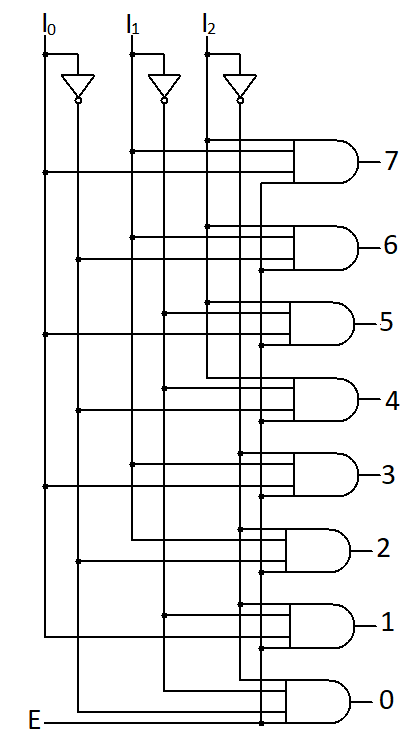
Hence, output of decoder is nothing but min term of its input.
3×8 decoder using 2×4 decoders
We can build a 3×8 decoder using two 2×4 decoders. We can find the number of lower order decoders that together can build a higher order of decoder using the formula given below.

So, we need 3 to 8 decoder which has 8 outputs by using 2 to 4 decoders which has 4 outputs. So, we need two 2 to 4 decoders.
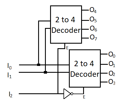
As you can see that input of both decoders is common and enable pin of both decoder is complement of each other. If I2 is ‘0’ then first decoder will be selected because not gate inverted the I2 input and first four outputs will be enabled. If I2 is ‘1’ then second decoder will be selected and next four outputs will be enabled.
4×16 decoder (binary to hexadecimal converter) using 3×8 decoders
As previously, we can implement 4 to 16 decoder by using either two 3 to 8 decoders or five 2×4 decoders. We will see both of that one by one but, first we will implement it using two 3 to 8 decoders. You can calculate the numbers of lower order decoders for implementing higher order of decoder using formula we previously discussed.
Number of 3 to 8 decoders for implement 4 to 16 = 16/8 = 2
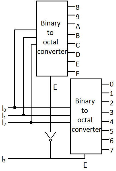
Logic for this diagram is same as previous.
4×16 decoder (binary to hexadecimal converter) using 2×4 decoders
To implement 4 to 16 decoder using 2 to 4 decoder we need five of them. Here that formula is not applicable. But this time we don’t need NOT gate. Maybe this is the reason why we need five 2 to 4 decoders.
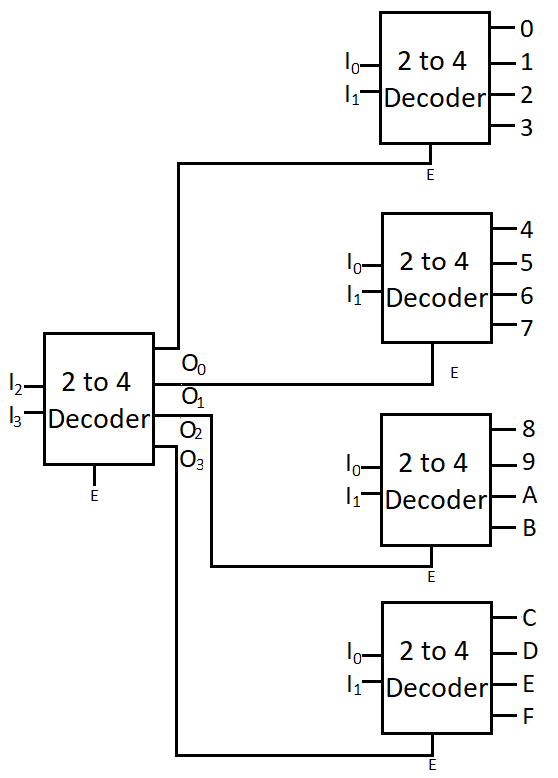
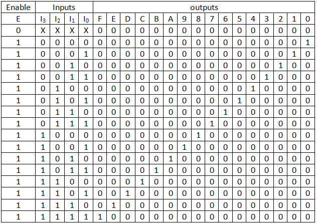
As per diagram you can see that a 2 to 4 decoder is used to select the other four decoders. Assume the case when I0 = ‘0’ , I1 =’0’, I2 = ‘0’ and I3 is also zero then top most decoder will be selected. By changing the value of I0 and I1 we can select any first four output. Now when I2 becomes ‘1’ then second decoder will be selected. Again by changing value of I0 and I1 we can select any next four output. Let’s understand this using truth table of 4 to 16 decoder.
Thank you very much
Thanks for your blog, nice to read. Do not stop.