MOSFET was developed to overcome JFET’s disadvantages like high resistance, moderate input impedance, and operational speed. It operates the same as the JFET but the difference is that its gate is isolated from its channel. It is also called IGFET (insulated gate field effect transistor). Its gate is isolated using metal oxide so this is called MOSFET (metal oxide semiconductor field-effect transistor). Like JFET, It also has three terminals- Gate, Drain, and Source. This is also a voltage controlled device like JFET.
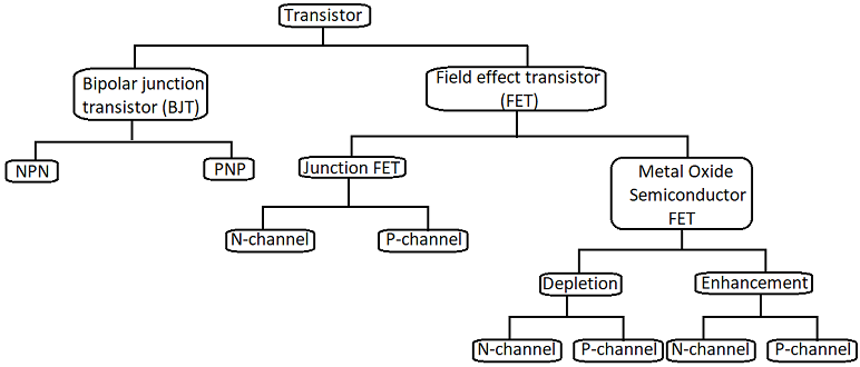
There are two types of MOSFET
- Depletion type MOSFET
- Enhancement type MOSFET
Table of Contents
Depletion type MOSFET
Let’s see the construction of MOSFET.
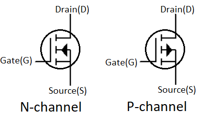
There are two types of MOSFET on the basis of its channel- N-channel and P-channel. Figure on the left side is the N-channel MOSFET and on the right side is P-channel. An N-channel MOSFET, the channel is made up of an n-type semiconductor which is fabricated on a p-type substrate. Source and drain are connected to the channel through metallic contact. Gate terminal is also connected to metallic contact but this metallic contact is isolated from the channel using metal oxide. This construction is reversed in P-channel MOSFET as shown. Due to the isolated gate, its input impedance is very large and there will not flow any current trough it. Now let’s see it’s working.
Working of depletion type MOSFET
A voltage supply is connected across an N-channel MOSFET’s drain and the source and gate to the source terminal are shorted as shown. So there will be zero volts on the gate. So, the drain side is more positive than the source. So, electrons will be attracted towards the drain terminal and a flow of electrons will establish from source to drain. But, the conventional drain current will flow from drain to source.
If we further increase the voltage across the drain and source current will also increase. But, after a certain value of voltage, if we increase the voltage even further, the current will still remain constant. This is also known as a drain to source saturation current (IDSS).
If we apply a negative voltage to the gate terminal then an electron will get accumulated on the metallic surface of the gate terminal. This will push the electron of the n-channel and attract the holes of the p-type substrate and then both will recombine. So, free electrons of the n-channel will reduce and the resistivity of the channel will increase. This way drain current will reduce. The rate of recombination of electrons and holes depends on the negative voltage applied.
If we apply a positive voltage to the gate terminal the minority carrier of the p-type substrate (which are electrons) will get attracted toward the channel. So, the number of charge carriers of the channel will increase. This will increase the flow of current even higher than drain to source saturation current.
All the voltages, current, recombination, and attraction minority charge carrier are reversed in the P-channel MOSFET (see characteristics graph).
Output characteristics of depletion type MOSFET
This is the output characteristic of an N-channel MOSFET. As shown in the graph if we decrease the gate voltage the drain current will also decrease.
This is the output characteristic of a P-channel MOSFET. As shown in the graph if we decrease the gate voltage the drain current will increase.
Symbols of depletion type of MOSFET
Enhancement type of MOSFET
It is almost the same as the depletion type of MOSFET. The only difference is that here channel is not present initially but when we apply a voltage to its gate terminal, it creates the channel. Let’s see how.
If we apply a positive voltage on the gate terminal of MOSFET, it will repel the holes and attract the electron. In this process, electrons and holes will recombine. But, if the voltage is high then they will overcome the recombination and electron will start accumulating on metal oxide. It will create a channel for current flowing. This is called the inversion layer and the voltage (VGS) at this inversion layer is just created is called threshold voltage (VT). As we increase the VGS width of the inversion layer will increase.
If you notice there are two p-n junctions in MOSFET. The first junction is on the p-type substrate and n-type semiconductor of the drain terminal. The second junction is on the p-type substrate and n-type semiconductor of the source terminal. Both junctions are in reverse bias so, there will be a depletion region on both junctions.
If VGS > VT and we connect a voltage supply across the drain and source, the source side will be more positive than the drain side. P-n junction on drain side will more reverse bias so, the depletion width of drain side will wider. That means their channel will narrow because the depletion width is wider so, fewer electrons will cross the barrier and accumulate on the gate side.
As we keep increasing the voltage on the drain side depletion width will get wider and wider and the channel will get narrower at the drain side. And at a certain voltage, this channel will not compete for the path between drain to source. This condition is known as pinch-off condition and the voltage (VDS) at this occurred is known as saturation voltage (VDS(sat)).
VDS(sat) = VGS -VT
That means the pinch-off condition will occur when the difference between the gate and drain terminal is equal to the threshold voltage. At the pinch-off condition, a constant current flows because electrons can cross the depletion region due to electrical force. This current is known as saturation current.
Output characteristics of enhancement type MOSFET
This is the output characteristics of N-channel enhancement type MOSFET. This graph shows that if we increase the gate voltage drain current will also increase.
This is the output characteristics of P-channel enhancement type MOSFET. This graph shows that if we decrease the gate voltage drain current will also decrease.
Symbols of depletion type of MOSFET
They are almost identical to depletion type MOSFET symbols. Here discrete line indicates that there is no direct connection of drain to source.
Linear or ohmic region
The left side of the locus of the VDS(sat) curve is the linear region. In this region, a MOSFET can be used as a voltage controlled resistor. Keeping the value of VDS fixed and by changing the gate voltage we can change its resistance. It also works as a “switch on” in this region.
Cut-off region
If VGS
Saturation region
Right hand side of locus of VDS(sat) curve is the saturation region. MOSFET works as an amplifier in this region.
VDS >= VGS – VT
MOSFET as a switch
The most popular type of MOSFET is the enhancement type. So, we will be taking an example of enhancement type MOSFET as a switch. MOSFET operates like a switch in its linear region and cut-off region. Let’s understand how?
Here both N-channel and P-channel MOSFETs are shown a switch. Giving high enough pulse voltage to the gate of an N-channel MOSFET so that it can work in the linear region, we can use it as an “ON” switch. And connecting the gate to the ground so that it is in the cut-off region, we can use it as an “OFF” switch. In the P-channel MOSFET giving the gate a high voltage will turn it off and by connecting it with the ground it turns on.
MOSFET as an amplifier
The circuit shown above is the popular common source (CS) amplifier using MOSFET. Here R1 and R2 are used to bias the MOSFET. There are more other ways to bias the MOSFET. Biasing is done in a transistor to power it and keep it in working condition so that our AC signal doesn’t get distorted. In this circuit the biasing technique is used is voltage divider biasing. Two capacitors that are used is called decoupling capacitor and their function is to remove any DC offset from the AC signal.
There is not any current flowing through the gate terminal. The only current flow in the circuit is VDD to the ground and that is the drain current. This current also flows through the resistor Rd, drain to source of MOSFET and resistor RS. So, by applying the KVL in this loop we can find values of resistors and outputs drain to source voltage (VDS).
Drain current that is flowing through the MOSFET is
Where:
IDSS = drain to saturation current
VGS = gate to source voltage
VP = pinch-off voltage
By applying KVL
VDD – IDxRd – VDS – IDxRS = 0
VDD – VDS – ID(Rd + RS) = 0
VDS = VDD + ID(Rd + RS)
(using the formula above we can calculate output voltage)
(Rd + RS) = (VDD – VDS)/ ID
Rd = (VDD – VDS)/ ID – RS
RS = VRS/ID (VRS is voltage across resistor RS)
(using the formulas above we can calculate value of resistances)