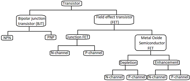
JFET is an active device that has three-terminal. This is a voltage controlled device. This is why we call it a junction field-effect transistor. Unlike BJT which is a bipolar (means the main collector to emitter current flow through both p-type and n-type semiconductor) device, JFET is a unipolar (current flows through either n-type or p-type semiconductor) device. If the current from source to drain passes through an n-type semiconductor then this is the N-channel JFET otherwise it is P-type.
In BJT we have seen that collector to emitter current is proportional to base current and that makes a BJT current controlled device. BJT can switch a larger amount of current source with a small amount of base current. But, in the case of JFET drain to source current is proportional to voltage to its gate. Hence it is a voltage controlled device.
JFET is more efficient than the BJT and it can perform all the operations that a BJT can. It is widely used in digital CMOS chips because it is efficient, fast, cheap, and small in size.
Table of Contents
JFET construction
The figure shown above is an N-channel JFET. There are three terminals shown in the figure- drain, source, and gate. Drain and source are connected to the both ends of the n-type semiconductor block through which drain to source current passes. To control that drain to source current two p-type blocks are fabricated near this n-type channel at both ends and it is connected internally which is the gate terminal of JFET. Together they form two p-n junctions and hence there is created a small depletion region. By biasing them we can control depletion width and then the amount of current flowing from drain to source. All structure is reversed in the P-channel JFET.
JFET working
Let’s consider an N-channel JFET. If we connect drain and source to a voltage supply (VDS) and short gate to source as shown. A current starts flowing from drain to source (drain current). By applying a voltage to the gate and source we can control this current.
If we increase the drain to source voltage further, both p-n junctions will be getting more reverse biased, and the depletion region will get wider. Resistivity of channel will also keep increasing. So, drain current will not increase linearly (See JFET output characteristics).
You can see that depletion width is wider at drain side and narrow at the side of the source. The reason behind it is the resistivity of n-channel block. As we connect a power source to an n-type block, the drain current will start flowing and there will be a voltage drop across it. The more the resistance more the voltage drop will be. The drain side will be more positive than the source side. So the junction biasing will be more powerful on the drain side.
If we further increase voltage across drain and source of JFET, a moment will come when both depletion regions will touch each other. This condition is called the pinch-off condition. The voltage between drain and source (VDS) at this occurs is called the pinch-off voltage (VP). And there will not any flow of current through the drain to the source.
If there is no flow of any current through the channel. There will not any different voltage levels across the channel. So depletion region will reshape itself and its width will be equal all around the junctions. Then the channel will open again. This will allow drain current to flow again.
As we considered previously that there will not flow any drain current after pinch-off that was not right. Rather this is the maximum current (saturation region) which can flow from drain to source. If we increase the VDS even further the current will still constant. This is the maximum current at VGS =0 and VDS > VP and it is known as a drain to source saturation (IDSS) current. In the case of P-channel JFET, these considerations are reversed.
But when we apply a negative voltage across gate to source the depletion region is getting wider even if the drain to source voltage is constant. By this way we can control the current flowing from drain to source.
JFET output characteristics
This is the output characteristic graph of N-channel JFET. This characteristics graph shows the relation between the drain current (ID), drain to source voltage (VDS) and gate voltage. As you can see in the characteristics, JFET acts like a resistor, at low voltages. But, as we keep increasing the voltage VDS drain side will get more and more positive and the depletion region will keep increasing so, the resistive property of the channel will keep increasing. After the pinch-off drain, the current ID will become constant. This graph also shows that if we give negative voltage to its gate-drain current will decrease. If we decrease voltage to its pinch-off voltage, JFET will be in cut-off region. No current will flow through the drain to the source.
This is the output characteristic graph of P-channel JFET. This characteristics graph shows the relation between the drain current (ID), drain to source voltage (VDS), and gate voltage. Here drain to source voltage is reversed. Now drain current will flow from source to drain. This graph shows that if we give positive voltage to its gate-drain current will decrease.
Let’s understand all the regions.
Ohmic region
This is the region where JFET acts like a voltage controlled resistor. By keeping the VDS constant and changing VGS we can control the resistance of JFET.
Saturation region
In this region, JFET works like a constant current source because in this region no matter how much we increase the voltage VDS, drain current will not increase. But, we cannot increase the voltage VDS to a certain value otherwise JFET will breakdown and this is called the “Breakdown region”. By keeping the VDS above the pinch-off voltage and changing the gate to source voltage (VGS) we can change the constant current value. In this region, JFET can be operated as an amplifier as well. To operate JFET in this region VDS should greater than that parabolic curve (right hand side of that curve for both type) shown in the characteristic graph and |VGS| should be smaller than the pinch-off voltage (|VP|).
Cut-off region
When the gate to source voltage is equal to pinch-off voltage, there will be almost zero current flowing through the drain to source or source to drain. This region is called cut-off region.
Symbol of JFET
We know that JFET has three terminal- source, gate and drain. Let’s see how to represent those to represent a JFET.
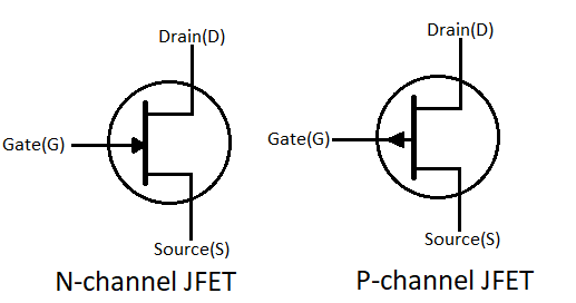
Symbols for both types of JFET are almost identical except the direction of the arrow. The direction of arrows shows the direction of current.
Drain current in saturation region
Let’s see how we can calculate the drain current of a JFET.
Where:
ID = drain current
IDSS = drain to source saturation current
VGS = gate to source voltage
VP = pinch-off voltage
As you can observe that if VGS is zero, drain current is equal to IDSS current which is the maximum current through a JFET. And if VGS = VP, drain current is zero which is the cut-off region.
JFET biasing
Biasing in a transistor is done to power it. Biasing keep it in working condition. Otherwise transistor will take power from the signal we have applied to it and signal will get distorted. So, we bias transistors to detect any change in AC signals and amplify them.
JFET fixed bias configuration
The circuit shown above is the fixed bias configuration of JFET. This is used for the amplification of AC signals. This circuit is powered using two voltage sources. VDD is connected across drain to source using a series resistor RD and VGG is connected across gate and source using a series resistor RG. since no current is flowing into gate terminal so, there will no voltage drop across resistor RG, that means VGS = -VGG. If there is any change in voltage Vi, this will be directly applied to the gate terminal. Those capacitors are for removing any DC offset from input and output. Now if we somehow find the drain current ID we calculate the voltage drop across RD (VRD) and VDS.
As we know that drain current is
We can find VDS by applying KVL in the outer loop.
VDD – VRD – VDS = 0
VDS = VDD – VRD
VDS = VDD – ID´RD
JFET in self bias configuration
In self bias configuration JFET needs only one power source to operate. It takes VGS from resistor RS. when drain current flow, it also flows through resistor RD. so, there is some voltage drop across the resistor (VRS) and it depends on how much current is flowing. So, this way JFET stabilizes its operating point.
VGS = -VRS
VGS = -ID´RS
VDD – VRD – VDS – VRS= 0
VDS = VDD – VRD – VRS
VDS = VDD – ID( RD – RS)
Voltage divider bias of JFET
There is one more configuration of JFET called voltage divider bias. In this configuration a divided voltage of VDD is given to the gate terminal of JFET.