In this post, I will explain how a diode works and we will see its construction. But before that, it is necessary to know about p and n types of semiconductors and the formation of the p-n junction.
Table of Contents
p-n junction
The p-n junction is the basic unit of many semiconductor devices such as diodes, transistors, etc. Understanding the behavior of the junction is extremely important for the analysis of other semiconductor devices. Now we will try to understand how a junction is formed and how a junction behaves under the influence of externally applied voltages (also called bias).
Formation of p-n junction
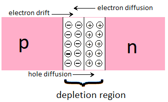
There are two important processes at the time of forming a p-n junction – Diffusion and Drift. We know that the concentration of electrons (the number of electrons per unit volume) in an n-type semiconductor is higher than the concentration of holes.
Similarly, in p-type semiconductors, the concentration of holes is higher than the concentration of electrons. At the time of the formation of the p-n junction, and due to the concentration gradient at the ends of the p- and n- region, the holes diffuse from the p- region to the n- region (p → n), and electrons diffuse from the n- region towards p-region (n → p). Due to this motion of the charge carriers, a diffusion current flows through the joint.
When an electron diffuses from p to n, it leaves an ionized donor behind it on the n-plane. This ionized donor (positive charge) is fixed due to bonding by the atoms around it. As the electrons diffuse towards n → p, a layer of positive (or positive space – charge region) develops on the n region of the joint.
Similarly, when a hole diffuses towards p → n due to concentration gradient, it leaves behind it an ionized receptor (negative charge) that is immobile.
As the holes diffuse, a layer of negative charge (negative space-charged region) develops on the p-region of the joint. This space-charge region developed on both sides of the junction is called the Depletion region.
This is because the electrons and the holes that participate in the initial motion across the junction depress the area of its free charge (Figure below). The thickness of this neck area is one-tenth of a micrometer.
Due to the positive space-charge field on the n – region of the junction and the negative space-charge field on the p region, an electric field is generated from the positive charge on the junction towards the negative charge.
Due to this region, the electron of the p-region of the junction moves towards the n- region, and the hole of the n-region of the junction moves towards the p- region.
The speed of charge carriers due to this electric field is called drift. Thus a drift current that is opposite to the diffusion current begins to flow.
Initially, the diffusion current is high and the drift current is low. As the diffusion process progresses, the interstitial charge fields on both sides of the joint expand. This increases the intensity of the electric field, resulting in an increase in drift current as well.
This process continues until both these currents (diffusion current and drift current) become equal in magnitude. Thus a p-n junction is formed. In equilibrium, there is no net electric current at the p – n joint.
Due to the loss of electrons from the n-region and the receipt of holes in the p-region, a potential difference arises across the junction of both fields. The polarity of this voltage is such that it opposes the flow towards the charge carriers, resulting in a state of equilibrium.
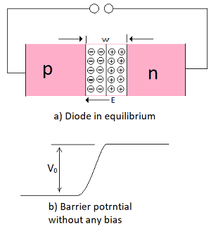
In the figure above, the junction is shown to be the difference between equilibrium and its ends. n-channel has lost electrons and the p-channel has gained electrons. Thus the n – substance is positive with respect to p – substance. Since the voltage tries to stop the movement of electrons from the n – region to the p – region, this voltage is often called the barrier potential.
Semiconductor diode
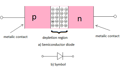
Semiconductor Diode [figure 3 (a)] is basically a p – n junction with metallic contacts at the ends so that no external voltage can be applied to the junction. This device has two terminals. Fig 3(b) shows the semiconductor diode symbolically.
According to the convention, the direction of the arrows represents the direction of the equilibrium barrier. (While the diode is in forward bias) the potential can be changed by applying external voltage V at the ends of the diode. p – n Position of the junction diode without bias is shown in Figures 2(a) and (b).
Diode in forward bias
When an external voltage V is applied between the two ends of a semiconductor diode, such that the plus side of the battery connects to the p-region and the minus terminal to the n-region [Figure 4(a) and (b)], then it is called forward bias.
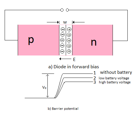
Most of the applied voltage lines are at the ends of the depletion region of the semiconductor diode and the voltage across the p-region and n-region of the junction is negligible (this is because the resistance of the lacy region, the region where there is no charge, is greater than the resistance of n-region or p-region).
The applied voltage (V) direction is opposite to the built-in voltage V. As a result, the thickness of the breastbone decreases, and the infarct height decreases [figure 4(b)]. The anterior bias has an effective barrier height (V0 – V).
If the applied voltage is small, the resistor potential will be only slightly lower than the equilibrium value, and only those charge carriers that were at the highest energy level will be able to obtain the energy needed to overcome the very small number of junctions, so low power the current will flow.
If we increase the applied voltage significantly, the insulator height will decrease significantly and more carriers will get the energy required to cross the joint. In this way, the electric current will increase.
Due to the applied voltages, electrons cross the n-plane deceleration region and reach the p-plane (where they are minority carriers). Similarly, the holes of the p-region cross the joint and reach the n-region (where they are minority carriers). This process, which occurs in a forward bias, is called Minority carrier injection.
At each region on the boundary of the junction, there is a significant increase in minority carrier concentrations compared to concentrations of minority carriers located away from the junction. Due to this concentration gradient, the edges of the p-region are diffused and reach the other side of the p-region. Similarly, the n-region diffuses from the edge of the junction and reaches the other end of the n-region (Figure below).
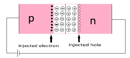
Due to this motion of charge carriers on both faces, an electric current starts flowing. The total forward diode current value is the sum of the hole diffusion current and the conventional current due to electron diffusion. The magnitude of this current is usually in milliamperes.
Diode in reverse bias
When an external voltage (V) is applied between the two ends of a semiconductor diode in such a way that it connects the positive terminal of the battery to the n-region and the negative terminal to the p-region [Figure 6 (a)], then the diode is called Reverse bias.
Most of the potential voltage applied is at the ends of the depletion region of the semiconductor. Here the applied voltage direction is the same as the direction of the resistor potential.
As a result, the height of the reticulum increases, and the width of the neck area increases due to a change in power. The reverse bias has an effective barrier height (V0+V) [Figure 6(b)]. It suppresses the flow of electrons towards n→p and the flow of holes towards p→n. Thus, in this case, the diffusion current is greatly reduced compared to the forward bias of the diode.
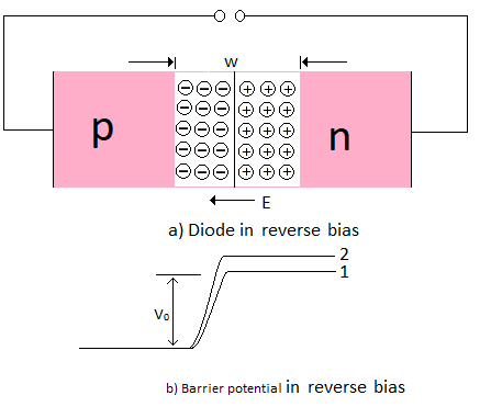
The direction of the electric field of the junction is such that if the electrons on the p-region or the holes on the n-region come close to the junction while doing their random motion, they will be sent to their majority field.
This drift of charge carriers will generate electric current. This drift current is of some A category. The reason for this being of little value is that the charge carriers move from their minor region to the majority of the region on the other side.
There is also a leakage current (usually in µA) in the reverse bias but it is negligible compared to the current (in mA) due to the intercalated carriers. Reverse current is not highly dependent on the applied voltage. A small voltage is sufficient to transport minor carriers from one region to another. The current is not limited by the result of applied voltage but is limited by the concentration of minority carriers on both sides of the joint.
In a reverse bias, up to a critical reverse voltage, the current does not depend on the voltage in a significant way. This voltage is called Breakdown voltage (Vbr). When V = Vbr then the diode backward current increases rapidly.
Even with a small increase in bias voltage, the current changes drastically. If the backward current is not confined below the value allowed by an external circuit (specified by the manufacturer), the p – n junction will be lost. If even once it exceeds the allowed value, the diode is destroyed due to overloading.
This can also happen when the diode is in the forward direction and the inward current is higher than the allowed value. The circuit diagram for studying the V-I characteristic (divergence of current as a function of the applied voltage) of a diode is shown in 7(a) and (b).
Voltage is connected to the diode via a potentiometer (or current controller) that allows the voltage to be applied to the diode. The value of current is noted for various values of voltages. A graph between V and I, as shown in Figure 7(c) is obtained.
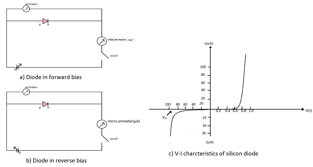
Note that we use millimeters for the forward bias measurement because the required current is high whereas in reverse bias a microammeter is used to measure less current.
In (fig 7) we can see that in the forward bias the current initially rises very slowly, almost negligible until the voltage on the diode exceeds a certain value. After this characteristic voltage, a slight increase in the diode bias voltage leads to a significant (exponential) increase in the diode current. This voltage is called Threshold voltage or cut-in voltage.
The value of this voltage for germanium diode is ~0.2 volts and for silicon, diodes are ~0.7 volts. In reverse bias, the current for the diode is very low (~µA) and remains almost constant with the change in bias. This is called Reverse saturation current.
Simple-purpose diodes are not used beyond the saturated current field. The above discussion shows that the p – n diode basically restricts the flow of current in only one direction (forward bias). The forward bias resistance is less compared to the reverse bias. This property has been used to characterize alternating (ac) voltages, which are explained in the next section.
For the diodes we define another physical amount, called dynamic resistance, as “the ratio of the small change in the voltage DV to the small change in the current and the DI”:
Application of diode as rectifier
In the V – I characteristic of a diode, we see that it allows current to flow only when it is biased. So, if an alternating voltage is applied at the ends of a diode, current will flow in the circuit only in that part of the cycle when the diode is biased forward. This property of a diode is used to direct the alternating voltage and the circuit used for this function is called a rectifier.
Half wave rectifier
If a reversible (ac) voltage at the ends of the diode is applied in series with a connected load resistance RL, then at the ends of the load only in the half cycle of the ac input in which the diode is facing forward, a pulsating voltage will be visible. This type of electrical circuit shown in figure 8 is an electric circuit called a half-wave rectifier circuit.
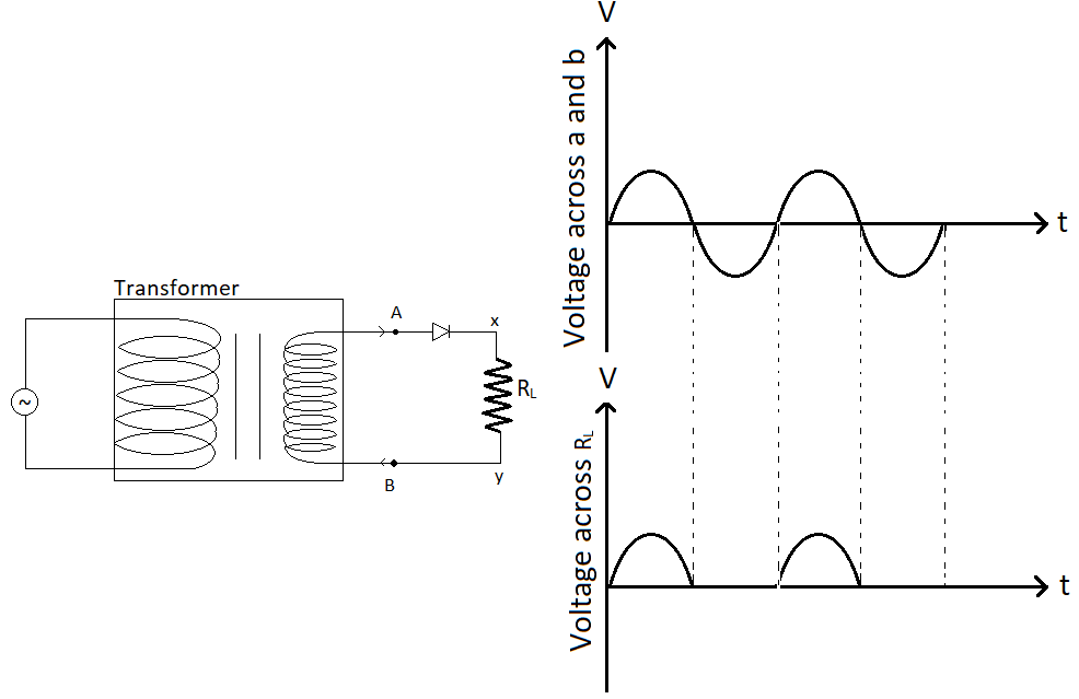
The secondary coil of the transformer supplies the desired ac voltages at terminals A and B. When the voltage at A is positive, the diode is in forward bias and conducts electric current.
When the voltage at A is negative, the diode is in reverse bias and does not conduct electricity. In the reverse bias, the saturated back current of the diode is negligible and can be considered zero for practical purposes. (The value of the diode’s direct breakout voltage must be much higher than the peak ac voltage on the secondary coil of the transformer so that the diode is protected from direct breakage).
Therefore, in a positive half cycle of ac voltages, the electric current will flow through the load resistance RL and we get the output voltages as shown in Figure 8 (graph). But electric current will not be received in the negative half-cycle. In the next positive half cycle, we will then get the output voltage. Thus, although the output voltage is still variable, it is called rectangular due to being restricted in only one direction. Since we are receiving the output voltage is only one-half cycle of ac wave, this circuit is called a half-wave rectifier.
Full wave rectifier
The circuit is shown in Figure 9 (a) using two diodes provides a circuit that gives corresponding output voltages in both the positive and negative half cycles of the ac cycle. That is why this circuit is called a full-wave rectifier.
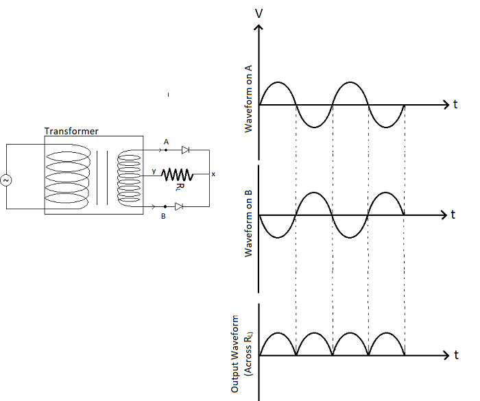
In this, the n – regions of both diodes are joined together and the output is obtained between this common point of the diodes and the midpoint of the secondary coil of the transformer. Therefore, for a full-wave rectifier, a tapping point is provided in the middle of the secondary coil of the transformer and hence this transformer is called a center-tap transformer.
As is clear from Figure 9(graph), the voltage indicated by each diode is only half of the total voltage from the secondary coil. Each diode represents only half a cycle, but two diodes are alternating cycles. Thus the output voltage obtained between the common point of the diodes and the fraction removal point of the middle discharge transformer is the absolute waveform voltage.
(Note that there is also another circuit for full-wave rectifier that will not require a mid-discharge transformer but needs four diodes called bridge rectifiers).
Suppose at some moment the input voltage at A of the middle ejector is positive. It is clear that the voltage at B is negative due to the phase being inconsistent at this moment as shown in Figure 9(c). Therefore, diode D1 conducts electric conduction via a forward-facing bias (while D2 does not conduct due to a transverse bias).
Hence, in this positive half cycle, we get an output current (and the output voltage at the ends of the load resistance RL) as shown in Figure 9(graph). Similarly, at any other moment, when the voltage on A becomes negative then the voltage on B will be positive.
Therefore, diode D1 does not conduct, but diode D2 conducts. Thus the output current (and the output voltage at RL) is also found in the negative half-cycle of the input ac. Thus, we get the output voltage in both the positive and negative half-cycles (that is, in other words, at the time of the full-wave). Clearly, it is a more efficient circuit than a half-wave rectifier to obtain direct voltages or currents.
The optimum voltage obtained in this way is of a half sinusoid shape. Although it is unidirectional, its value is not constant. A capacitor is usually connected at the ends of the output terminals (lateral to the RL) to obtain the dc output from the pulsating voltage. This is called a capacitor filter.
Read the post on the capacitor.
I blog quite often and I truly appreciate your information. Your article has truly peaked my interest.
I am going to take a note of your website and keep checking for new details about
once a week. I subscribed to your RSS feed too.